The combination of different analytical methods within one instrument is of great importance for the simultaneous acquisition of complementary data. The FusionScope seamlessly combines two of the most powerful microscopy methods – atomic force microscopy (AFM) and scanning electron microscopy (SEM) – to allow completely new insights into the micro- and nanoworld using true correlative microscopy.
In static mode, or contact mode, the tip is in continuous contact with the surface of the sample and follows the topography closely in the repulsive regime. Typically, the cantilever is operated in deflection feedback mode. The set cantilever deflection relates to how hard the tip pushes against the surface and therefore determines the force load between tip and sample. For contact mode, long and soft cantilevers with lower force constants typically are used.
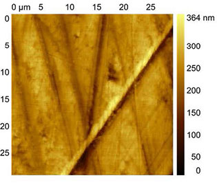
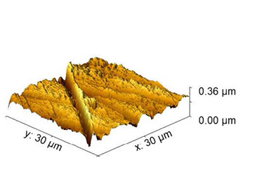
In dynamic mode, also called intermittent contact or tapping mode, the cantilever is oscillated near its resonance frequency. When the tip comes close to the surface, the interaction between the tip and the sample causes the amplitude of the oscillation to change. As the cantilever is scanning over the sample, the height is adjusted to maintain a set cantilever oscillation amplitude. An AFM image is therefore produced by imaging the force of the intermittent contacts of the tip with the surface. The user can fine tune the interaction between the tip and the sample working in both attractive and repulsive regimes. Since this interaction with the surface is rather gentle compared to static imaging mode, it can better preserve the sharpness of the AFM tip.
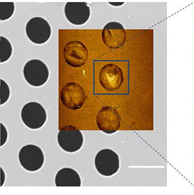
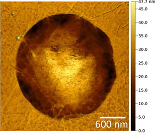
The Finite Impulse Response Excitation (FIRE) mode is a novel off-resonance intermittent contact scanning force microscopy technique. The FIRE mode is based on the observation of the cantilever signal in a frequency domain that is above the drive frequency but below the resonant frequency of the cantilever. The drive is provided by periodic excitation of the Z-flexure, which brings the cantilever tip periodically into contact with the sample. Comparison of the excitation profile to the cantilever deflection allows the gate array electronics to extract sample stiffness and tip adhesion in real time. Using this technique, when the tip is at a distance from the sample, background signals due to long range interactions can be measured and subsequentially subtracted from the measurements.
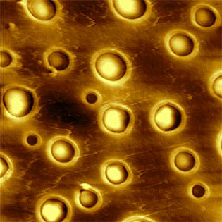
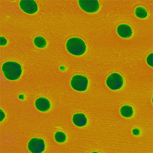
Standard Conductive AFM (C-AFM) works in static or contact mode by simultaneously measuring the sample topography and the conductive properties of the sample using a sharp conductive tip. The cantilever tip is in constant contact with the surface while applying a defined bias voltage between the tip and the sample and measuring the current flow. In this way a current or conductivity map of the surface can be created. In addition, single point IV curves can be recorded to probe the detailed electrical properties at user defined positions.
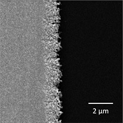
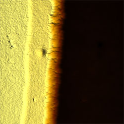
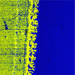
Electrostatic Force Microscopy (EFM) is a phase imaging mode used to study imaging variations in the electric field of the sample substrate and therefore study the surface potential and charge distribution. The EFM mode is the electrical equivalent to Magnetic Force Microscopy (MFM). Like MFM, the EFM measurement is typically done in a two-pass procedure. First the AFM tip is in contact with the surface measuring the topography in dynamic mode. Then in the second pass the tip is lifted by a user defined value (typically ranging from a few to tens of nm) and follows the topography of the surface in lift-mode. During the second pass a DC bias is applied between the conductive cantilever tip and the sample enabling the measurement of the long-range electrostatic interaction forces in combination with the sample topography.
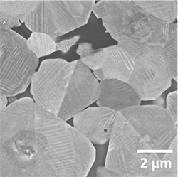
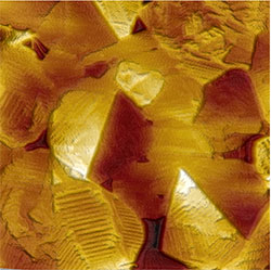
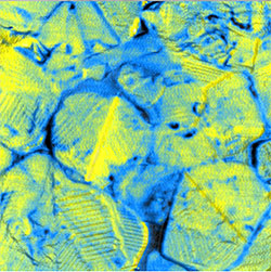
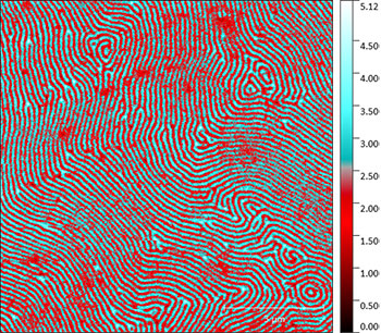
Magnetic Force Microscopy (MFM) is a phase imaging mode used to study the properties of magnetic materials using a magnetic AFM tip. The tip of the cantilever in atomic force microscopy generally experiences forces originating from the surface of the sample being measured. As a result, the structures shown are a product of the physical topography of the sample surface. However, by using different cantilevers, other characteristics of the sample can be detected and measured.
The simplest method to do this is a two-step procedure. The tip is drawn across the sample line by line and each of the two steps is applied to each line. In the first step, the topography of the sample surface is measured "normally" in AFM mode. In the second step, the same line of the sample is measured again, but the topography of the surface is traced at a defined distance above the surface so that phase shift and amplitude can be recorded.
Due to the distance to the surface, the tip of the cantilever experiences no interactions with short-range forces of the surface in the second step, but only with long-range forces that are still "visible" at this distance. Long-range forces are, for example, magnetic interactions. If the cantilever used has a permanent magnetic tip, these magnetic interactions can be mapped with this method.
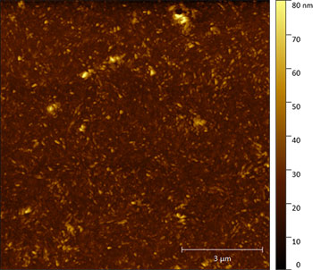
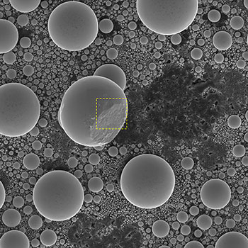
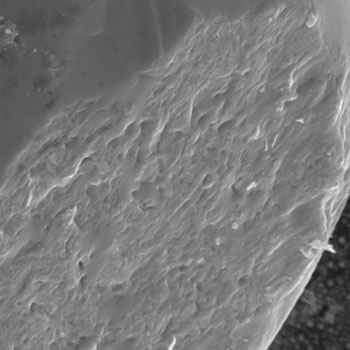
Using its focused electron beam, FusionScope can achieve high-resolution topographic imaging from the surface of your sample. In fact, with its highly surface-sensitive SE mode, FusionScope can collect topographic information from within a few nanometers of the surface.
How does FusionScope obtain this information? Through the use of Secondary Electrons (SE), which are lower energy (< 50 eV) electrons that have a limited escape depth (< 2nm). Thus, only the ones from the sample surface manage to emerge from the material. This allows for achieving very high topographic resolution in the SE mode with low beam energies (< 10 kV), with the additional benefit of reducing the damage caused by high energy beams. Since the SE yield (emission rate) is high, this mode also provides a better signal-to-noise ratio (SNR). Overall, this mode offers a good compromise of high resolution, fast and non-destructive imaging for dimensional analysis.
Resources
Company
Quantum Design, Inc.
10307 Pacific Center Court
San Diego, CA 92121
USA
+1 800-289-6996
+1 858-481-4400
Fax: +1 858-481-7410
This website may use cookies to ensure you get the best experience on our website.
View our Privacy Policy.

