By combining the complementary strengths of SEM and AFM, FusionScope opens the door to a whole world of new application possibilities.
Use the FusionScope for detailed Material Characterization of your samples and perform correlative analysis of their structural, mechanical, electrical, magnetic, and chemical properties on exactly the region of interest.
Whether you are looking for high-level Quality Control of component parts or want to perform Failure Analysis on electrical components or semiconductor devices, FusionScope will help you to get the job done. Benefit from the fast and intuitive workflow to extract the data you are looking for.
Combining high-resolution SEM and state-of-the-art AFM you can easily characterize Nanostructures such as nanowires, 2D-materials, and nanoparticles. FusionScope gives you full control to locate the Nanostructures and perform the measurements of your choice.
Using FusionScope in Life Science applications allows you to acquire the nanoscale morphology of biological samples accurately and easily. Especially for hard-to-reach sample areas or very small features, FusionScope allows you to characterize physical properties such as 3D topography, stiffness, and adhesion with the highest precision.
Modes: SEM, AFM Topography and Phase, MFM
Sample: Artificial Spin Ice
Spin ice is a fascinating and unique state of matter within the field of condensed matter physics, characterized by its magnetic frustration and emergent phenomena. In spin ice materials, the magnetic moments, or "spins," are arranged in a manner analogous to the positions of hydrogen atoms in water ice, hence the name. This arrangement leads to a highly degenerate ground state and the emergence of exotic excitations that mimic magnetic monopoles – entities long theorized in physics but never observed in isolation. The study of spin ice not only provides insights into fundamental aspects of magnetism and statistical mechanics but also has implications for the development of new technologies, such as advanced magnetic storage systems and quantum computing.
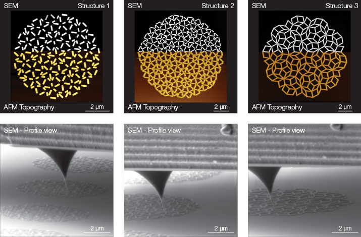
A sample of patterned Permalloy (Ni81Fe19) was used to demonstrate FusionScope's capability to provide correlative MFM and SEM analysis. Figure 1 shows the three different "Penrose patterns" that were analyzed. Such structures, where each nanorod is essentially a small ferromagnet, are potential candidates for ultra-high-density data storage devices. We fabricated high-aspect ratio magnetic tips using a 3D nano-printing technology. These 3D nano-printed tips are typically made of Fe or FeCo and allow tip radii of only 10 nm.
Using FusionScope's unified coordinate system in combination with Profile View, the cantilever can be easily navigated to the region of interest. This allows precise positioning of the magnetic cantilever tip on the different magnetic nanostructures (Figure 1, bottom row). Correlative SEM and AFM topography can be performed and directly correlated using the FusionScope software interface (Figure 1, top row).
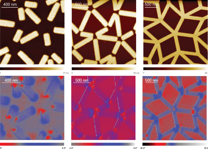
To study the artificial spin ice, we used dual scan MFM in lift mode with a typical lift height of 40 nm. As can be seen in Figure 2 (top row) the artificial spin ice is composed of structures with typical heights of 35 to 50 nm (depending on the specific structure). In all three different structures the measured intensity of the magnetic field changes at the vertices of the separated or interconnected nanorods (Figure 2, bottom row). These vertices with high intensities can act as hotspots where ferromagnetic switching of the nanorods can occur under an applied external magnetic field.
In summary, FusionScope provides an easy-to-use platform for correlative SEM and MFM analysis of magnetic nanostructures. Combining the benefits of a joint coordinate system, easy tip positioning via Profile View, and high-resolution MFM data with reduced phase artifacts enables new ways of characterizing your magnetic samples.
Mode: MFM
Sample: Duplex Steel
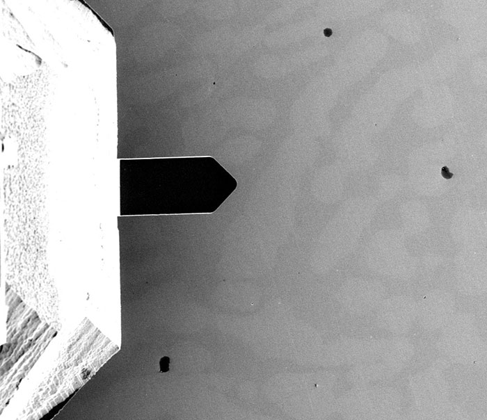
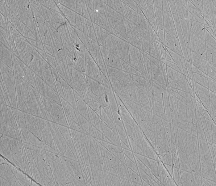
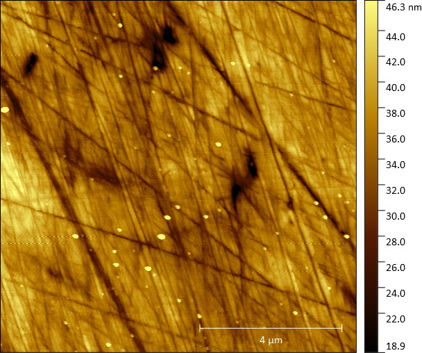
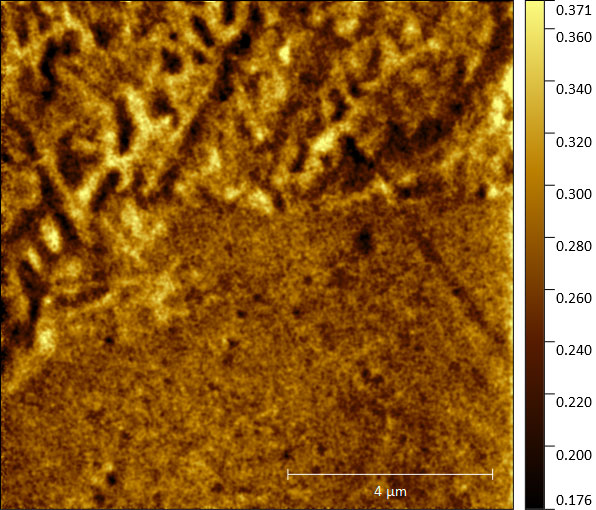
Duplex is a family of stainless steel grades that contain a mixture of austenitic and ferritic phases that provide higher mechanical strength and ductility compared to standard steel grades. In-situ Magnetic Force Microscopy (MFM) enables the detailed analysis of the magnetic properties of different types of duplex steel samples.
With the FusionScope the different phases of the steel surfaces can be visualized, and the cantilever is easily positioned at the grain boundary of two distinct phases. Using a magnetic cantilever tip the magnetic properties can be analyzed, and the ferromagnetic sub domains can be imaged with high resolution.
Mode: EFM
Sample: BaTiO3
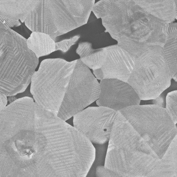
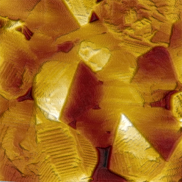
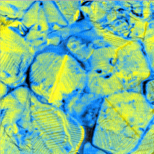
Barium titanate (BaTiO3) is a ceramic material exhibiting interesting optical, electrical, and thermal properties shifting it to the center of scientific attention. More recently BaTiO3 is gaining importance also for engineering applications. Ferroelectric BaTiO3 is a non-linear positive-temperature-coefficient (PTC) material and is used in resistors. Polycrystalline doped barium titanate exhibits a wide range of electrical resistance depending on the temperature which is employed in sensors and actuators.
The macroscopic electronic properties of polycrystalline BaTiO3 ceramics are governed by potential barriers forming between single grains. To reach a better understanding of the overall resistance of barium titanate it is essential to be able to characterize the potential differences in the crystalline material at the nanoscale.
This characterization can be done with Electrostatic Force Microscopy (EFM). It is widely used in electronics development to map electronic characteristics of complex, sub-micron electrical materials. FusionScope enables the possibility for in-situ EFM analysis. The high resolution of the SEM can be used to easily identify grain boundaries and perform the EFM analysis directly at the region of interest.
Modes: SEM, AFM Topography, EDS
Sample: Interlayer VIA Circuit


Failure analysis and quality control procedures are very important for determining errors in the manufacturing process and increasing yields of manufactured devices. This can be especially challenging in interlayer circuits, such as a VIA (Vertical Interconnect Access) circuit (Figure 1). In these cases, a three-part analysis using the correlated capabilities of SEM, AFM and EDS in the FusionScope can greatly increase knowledge about samples and help in their improved manufacturing.
First, the SEM is used to map the large area and identify potential spots of failure by providing detailed imaging of the overlay error that occurs when layers of material are misaligned, decreasing the contact area and potentially lowering the device performance or in some cases leading to failure. The SEM image also provides high-resolution lateral information on the X and Y axes, facilitating the precise measurement of overlay accuracy (Figure 2a).
FusionScope's unified coordinate system, along with the coordinates provided by the SEM, allow AFM measurements to be easily gained by executing an automated scan command. The complementary vertical surface information provided by the AFM data reveals the topographic details of the surface along the Z axis, which are not clear in the SEM image. In this example, the AFM reveals that the circuit line is thinned over the VIA, potentially contributing to an impaired electrical connection (Figure 2c).
The SEM (Figure 2a) and AFM (Figure 2c) images show an oval region in the center of the line, which might lead to the conclusion that the VIA covers this entire area, ensuring a proper electrical connection. However, the elemental information acquired by the EDS image (Figure 2b) reveals a higher concentration of aluminum (Al) at the upper central part of the oval feature, surrounded by silicon (Si). This indicates that the VIA is not centered and is smaller than the oval feature observed in the SEM and AFM images. By combining this with the topographic information from AFM (Figure 3) we can determine that the VIA only contacts the top Al line, where the line is thinned, indicating an even weaker electronic connection.

It would not be possible to fully understand the details of this failure without the correlated information from SEM, AFM, and EDS. This correlative approach allows for more precise identification and characterization of defects, improving diagnostic accuracy. This way, the weaknesses in the design and production process can be better identified. The ability to analyze failures rapidly and accurately can reduce downtime and costs associated with troubleshooting and repairs, ultimately enhancing the reliability and performance of electronic devices.
Modes: SEM, AFM Topography and Phase
Sample: Machined Gear & Micromotor Elements
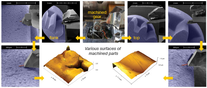
Material processing is key to achieving desired properties across a diverse range of applications. Surface properties, in particular, play a crucial role, and Atomic Force Microscopy (AFM) is the tool of choice for this task due to its capability for 3D metrology with nanometer spatial resolution. Moreover, AFM offers advanced modes that provide access to electric, magnetic, mechanical, optical, and thermal properties. Here, we highlight two examples that demonstrate the advantage of using FusionScope for easy and fast analysis.
First, consider machined gears produced through techniques such as casting, sintering, or direct CNC preparation. These gears often undergo stress tests to evaluate performance under different operating conditions, making it essential to characterize them before, during, and after these tests. Traditional AFMs struggle with this task due to difficulties in positioning the tip at areas of interest. FusionScope, however, excels by enabling SEM identification of these areas followed by precise tip approach made possible by the platform’s superb resolution and its 0-to-80-degree tilt angle of the sample and AFM scan head (Figure 1). These capabilities aid initial material processing, enable fast examination of surface properties, and help track wear effects.
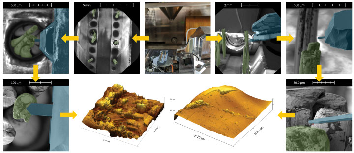
The second example involves a micromotor with rotors that are electrically conducted by brushes. Motor performance heavily depends on the interaction regions, making the characterization of both elements after stress tests crucial for identifying abrasive behavior and material cross-contamination. FusionScope’s combined SEM and AFM capabilities are ideal for positioning the cantilever on areas of interest, as seen in Figure 2. The morphological information gathered is essential for understanding wear and potential failure processes.
Modes: SEM, AFM Topography
Sample: Razor Blade
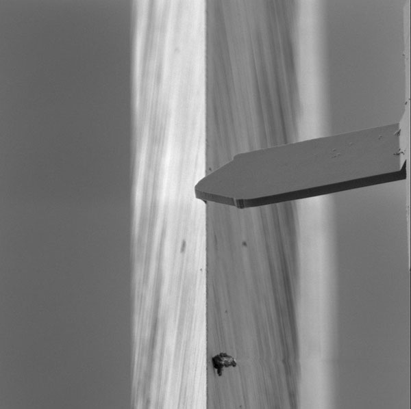
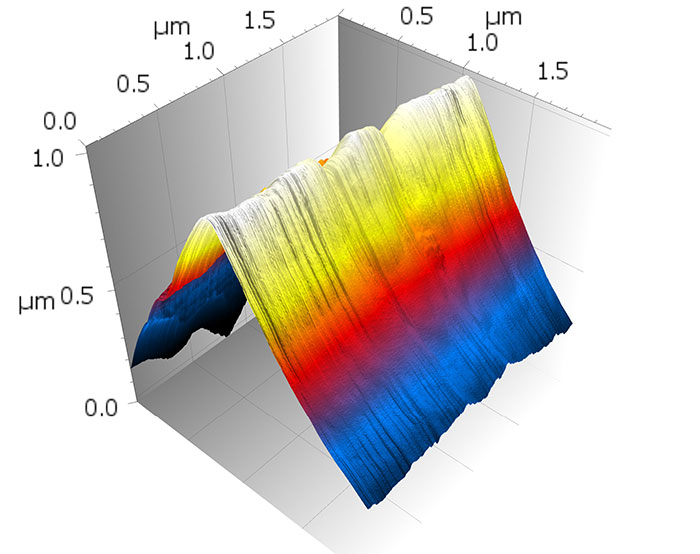
Typically, in atomic force microscopy, measurements of very pointed sample geometries are difficult. Firstly, due to the convolution of the geometry of the tip with the topography of the sample surface, but also the correct and reliable positioning of the tip over the sample is a challenge. SEM is used here to position the sample in the best possible way and to monitor the AFM measurement in real time.
A commercially available razor blade was installed in the sample holder with the aim of imaging the surface of the blade with the AFM and, in particular, determining the radius of the blade edge. The measurement comprises several steps: the coarse positioning, the fine positioning, the approach of the tip and finally the measurement of the topography. With the help of the fine positioning made possible by the SEM, different areas on the razor blade can be quickly selected and measured. Different material properties, such as a coatings applied to the razor blade, also can be compared. An important parameter is the radius of the razor blade, as well as the roughness of the surface.
Modes: AFM Topography, SEM
Sample: CPU Chip
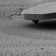
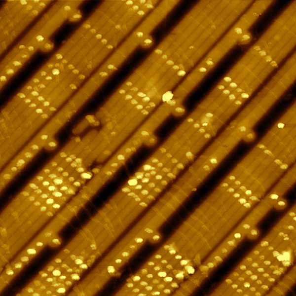
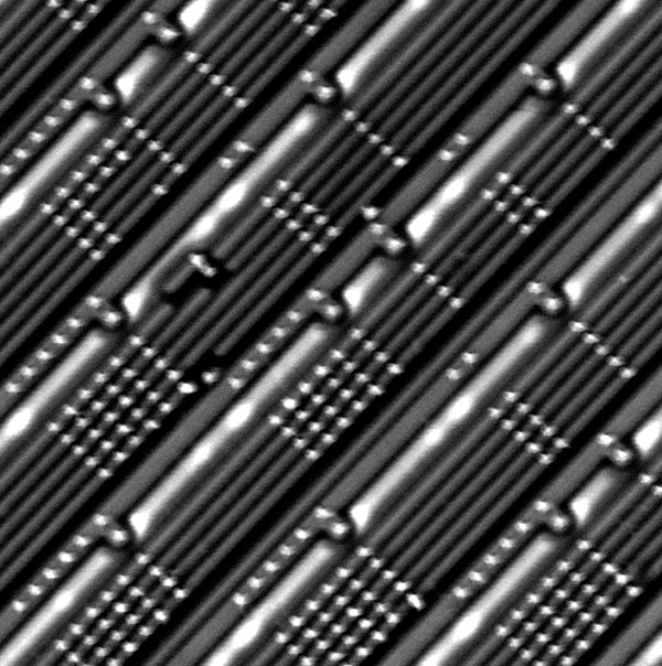
Detailed location and analysis of nanometer-sized structures is a challenging and time-consuming task for all AFM operators. The size reduction in recent generations of transistors creates especially high demands on quality control and failure analysis. With FusionScope and Profile View you can easily navigate the cantilever tip to the region of interest and perform high resolution AFM analysis of your sample. Measure the real 3D topography with sub-nanometer resolution or extract additional information using conductive AFM.
Modes: SEM, Force-Distance-Curves
Sample: 3D-Printed Nanopillars
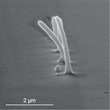
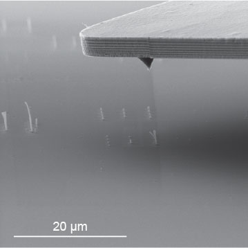
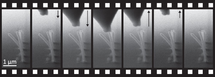
Characterizing the mechanical properties of 3D nanostructures, which have unique mechanical properties that can differ significantly from their bulk counterparts, is a crucial technique for advancements in nanotechnology, materials science, and various applied research fields. Understanding these properties is essential for their integration into nanoscale devices and applications, including sensors, transistors, and other electronic components. We analyzed the mechanical properties of 3D nanopillars (~200 nm diameter), fabricated using Focused Electron Beam-Induced Deposition (Figure 1). FusionScope’s correlative AFM-SEM integration along with Profile View enable nanometer accuracy in aligning the AFM tip when the trunnion is tilted at 80° (Figure 2). The force between the cantilever’s tip apex and the pillar is measured by the calibrated deflection of the cantilever. As the cantilever moves downward, the pillar bends until the exerted force reaches a set point. The cantilever then retracts, allowing the pillar to return to its original shape (Figure 3). The mechanical response of the pillar and the cantilever can be modeled using the calibrated cantilever data and its calculated stiffness (Figure 4).

Publication: A Highly Integrated AFM-SEM Correlative Analysis Platform
Modes: SEM, AFM Topography and Phase
Sample: Plasmonic Nanowires


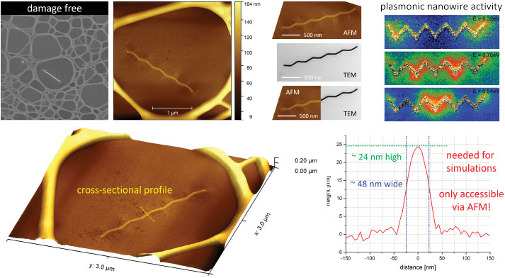
Plasmonic nanostructures exhibit unique optical properties that are determined by their shape, spatial orientation, and material composition. Precise control of nanostructure geometries is crucial for tuning their plasmonic response within various applications. Focused Electron Beam Induced Deposition (FEBID) is a promising technique for producing high-fidelity nanoscale architectures, offering high design flexibility and the creation of complex 3D nanostructures. In this example, FEBID was employed for the direct-write fabrication of planar Au nanowires, which were plasmonically characterized using scanning transmission electron microscopy-based electron energy loss spectroscopy (STEM-EELS) mapping measurements. These findings were complemented by corresponding plasmon simulations, validating the experimental data.
For the simulations it was crucial to access the real 3D morphology after STEM-EELS characterization. Since these measurements are typically performed on ultrathin membranes (sub-5 nm in this case), traditional AFMs are impractical due to difficulties in visually locating the nanostructures. FusionScope's Profile View offers a solution, as it allows for direct localization of the Au nanowires, enables precise tip positioning, and minimizes the risk of fracturing the ultrathin membranes during prolonged searches (Figure 1). The platform's excellent resolution provides reliable morphological data, as evidenced by a direct comparison between transmission electron microscopy (TEM) and AFM results (Figure 2). The obtained cross-sectional profile data serves as direct input for nanowire simulations of the very same structures, enabling direct correlation with STEM-EELS data for an iterative optimization of printing procedures.
Overall, FusionScope proves to be the ideal tool for complementing TEM studies, with the potential to provide additional magnetic, electric, or mechanical information that is partially inaccessible through TEM alone.
Mode: AFM Topography
Sample: Nanowires
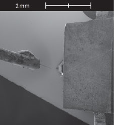
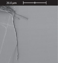
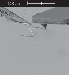

The detailed characterization of individual nanowires using conventional AFM in combination with an optical microscope is always a challenge, as single nanowires cannot be easily identified and imaged with this setup. Using Profile View in FusionScope allows one to overcome these limitations. The visibility of the cantilever tip in combination with the high-resolution SEM enables the user to navigate the cantilever precisely to the specific nanowire of interest. Once there, measurements such as topography and side-wall roughness, as well as mechanical and electrical properties, can then be obtained. This method gives the user a completely new and interactive way of performing nanowire measurements.
Mode: AFM Topography
Sample: Freestanding Graphene
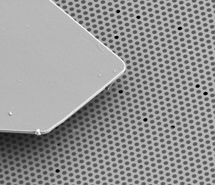
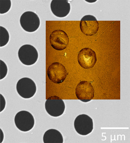
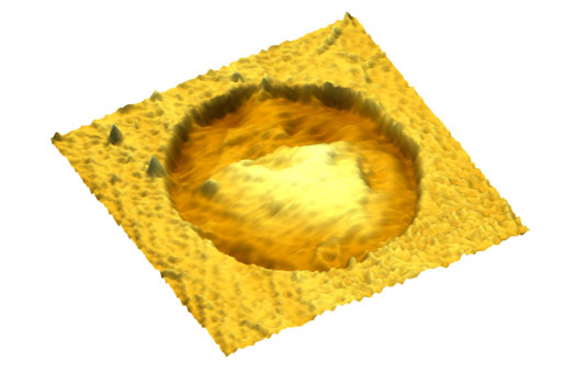
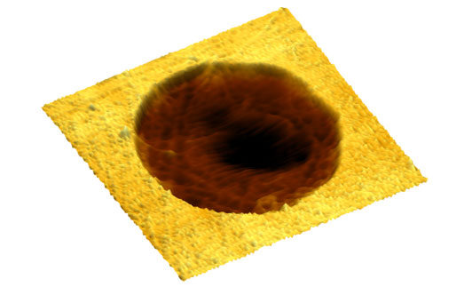
Freestanding suspended membranes of two-dimensional materials (2D) are of great interest for many applications ranging from nanoelectromechanical sensors to optical devices. Much of their characterization relies on scanning probe microscopy techniques such as atomic force microscopy (AFM). Unlike rigid samples, the suspended atomically thin 2D membranes are, however, flexible and do not remain mechanically undisturbed during AFM measurements, which can lead to a misinterpretation of actual membrane topography and nanomechanical properties. FusionScope can circumvent these shortcomings by visualizing the membrane deformation during the AFM analysis, which leads to a better understanding of the acquired AFM data.
Mode: AFM Topography, SEM
Sample: HOPG

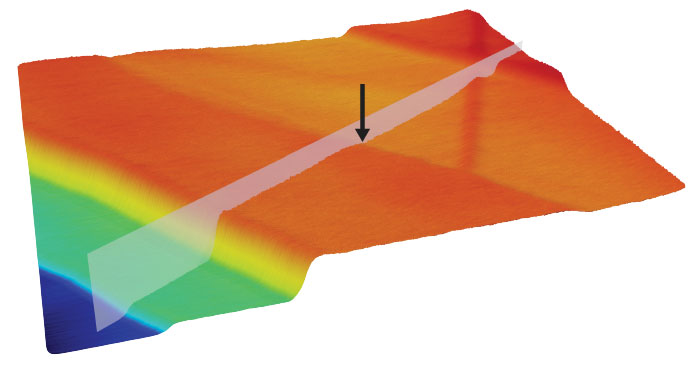
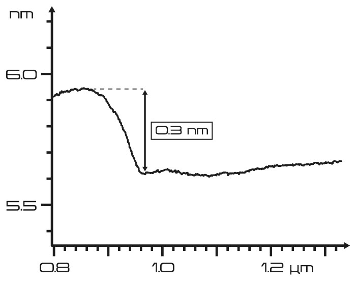
In order to detect the smallest changes in the properties of your sample surface the mechanical and electrical noise of your AFM system needs to be as low as possible. This becomes especially challenging in high-vacuum systems where you must consider noise sources such as the mechanical vibrations of turbo pumps (as an example). FusionScope offers you performance without compromise by giving you true atomic resolution for your AFM measurements. This is nicely demonstrated by measuring single atomic steps on highly pyrolytic oriented graphite (HOPG).
Modes: SEM, AFM Topography and Phase, EDS
Sample: Superparamagnetic Particles
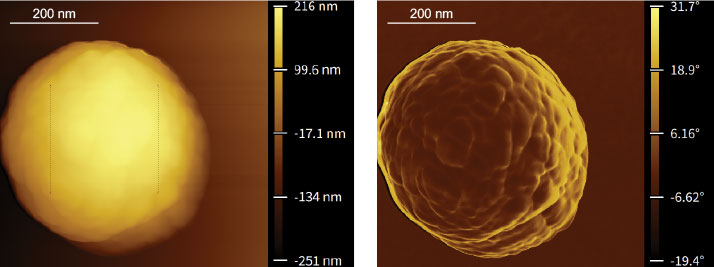
Nanoparticles (NPs) have broad applications in biological, medical, and pharmaceutical sciences, such as bio-separation, biosensing, diagnostics, and drug delivery. Because the functionality of NPs is highly dependent on their size, shape, surface, and material, the accurate characterization of particles is essential to their specific applications. And yet, the characterization of NPs can be challenging since different microscopy techniques are required to extract information, such as surface roughness and material composition. Furthermore, it is very challenging to measure sub-visible-wavelength sized particles accurately by optical methods.
For this example, we use carboxyl (COOH) group functionalized magnetic particles as a model system to demonstrate FusionScope’s imaging capability. The FusionScope allows us to image the particle’s surface with picometer resolution. The wide field of view of the SEM is employed to localize particles for AFM imaging. The topography and phase data from the AFM permit high-resolution inspection of the particle surfaces. We then use the correlated coordinate system and correlative in-situ measurement modes to capture relational AFM and SEM data. Higher-resolution AFM images from a single particle are shown in Figure 1. Finding particular particles of this size to take AFM data would be extremely difficult without FusionScope's correlated coordinate system and Profile View.

In addition, using EDS allows the identification of the iron core of the particles. The correlated SEM-EDS image gives insight into the size of the iron cores as well as the thickness of the organic polymer outer shells (Figure 2).
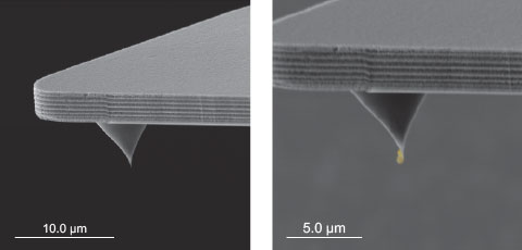
Worth noting is that AFM scans of finely sized particles such as these usually would be challenging because they can easily stick to the AFM tip, reducing the image resolution or leading to image artifacts. Using Profile View in FusionScope allows easy inspection of the AFM tip before, after, and even during the measurements (Figure 3).
Publication: Nanoparticle Characterization with In Situ AFM-SEM-EDS
Modes: SEM, AFM Topography and Phase, Force-Distance-Curves
Sample: Vitamin C Particles

Micro- and nano-sized particles have unique size-dependent properties crucial to pharmaceutical, electronics, and biomedical fields. Understanding and controlling these characteristics necessitate advanced techniques which often require jumping between multiple analysis tools. FusionScope enhances efficiency by seamlessly combining AFM and SEM, maximizing throughput with minimal resources.
This is demonstrated in the study of topographical and mechanical properties of individual Vitamin C particles. Different particle sizes ranging from 100 μm down to 10 nm can be identified using the SEM (Figure 1a). FusionScope’s correlated coordinate system allows for precise AFM tip positioning on target particles without the need for sample transfer (Figure 1b). SEM and AFM results can be directly correlated using the FusionScope software (Figures 1c and 1d).
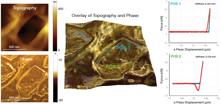
These measurements reveal particle roughness variations and provide 3D topography of samples. Furthermore, phase imaging and force-distance curves can be used to determine mechanical properties and identify surface contaminants. Figure 2 shows distinct phase contrast within the particle's crater structure, indicating contamination. The non-contaminated area exhibits greater hardness and less adhesion compared to the contaminated part.
FusionScope's Profile View ensures reliability, allowing users to observe cantilever movements during force-distance measurements, which helps avoid errors from sample deformation and ensures accurate mechanical property analysis.
Mode: AFM Topography
Sample: Bone
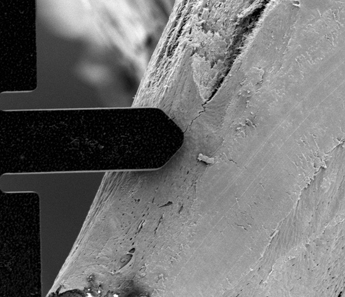

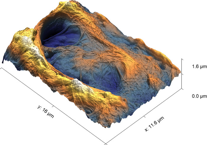
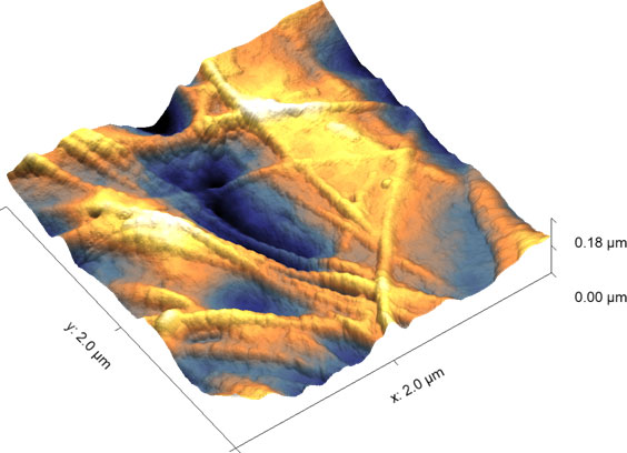
The correlative analysis of hard-to-reach sample areas is always a challenging task. One example is the analysis of bone tissue, especially the detailed measurements of lacunae and collagen fibers on the bone surface.
FusionScope offers a fast and easy identification and imaging of the lacunae structures. With the large field of view of the SEM the lacunae can be identified, and the cantilever positioned directly on the lacunae structures. Using the AFM, the real 3D topography of the lacunae and the collagen fibers can be extracted with sub-nm resolution.
Mode: AFM Topography, SEM
Sample: Seashell
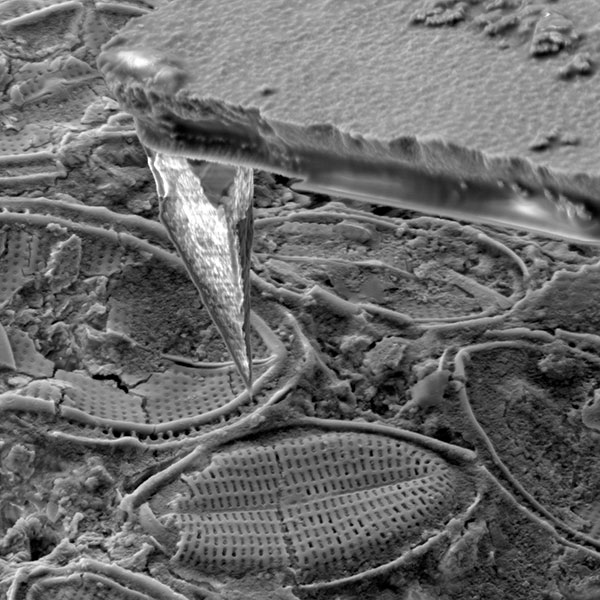
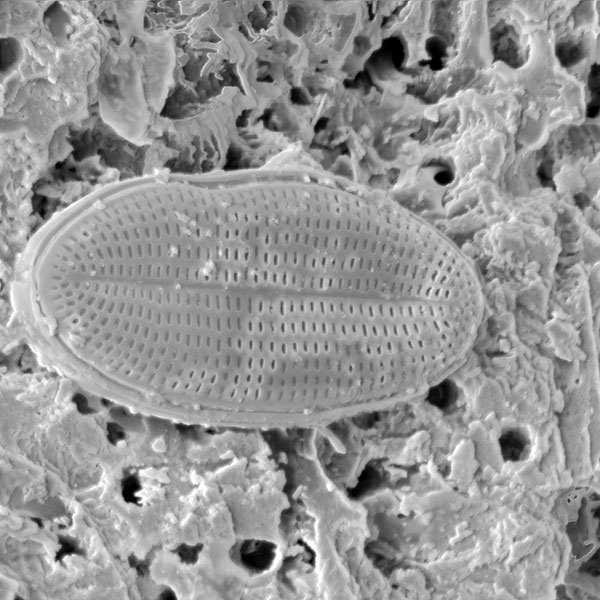
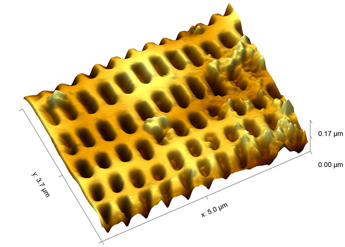
Diatom are fascinating unicellular organisms that make up a significant amount of the Earth's biomass. In this application we used the power of correlative microscopy to locate diatoms on the surface of a seashell using the high-resolution of the FusionScope SEM. With Profile view you can easily position the AFM cantilever tip on a diatom structure of your choice and perform a 3D topography analysis.
Resources
Company
Quantum Design, Inc.
10307 Pacific Center Court
San Diego, CA 92121
USA
+1 800-289-6996
+1 858-481-4400
Fax: +1 858-481-7410

